Overview
Our laboratory conducts research of spintronics. Spintronics is an academic field simultaneously utilizing two fundamental properties of electrons—charge (electrical property) and spin (magnetic property)—which have traditionally been treated separately. By exploring the novel physical phenomena that emerge from this simultaneous usage, we aim to contribute to the development of high-performance, energy-efficient electronics and advanced information and communication technologies. Specifically, our laboratory focuses on the following five areas, which interact with each other.
1. Non-Volatile Spintronic Memory Devices for Energy-Efficient Semiconductors
Semiconductor integrated circuits form the backbone of modern society, and their importance has been growing even more in recent years with the widespread deployment of AI. Semiconductors are also key to achieving carbon neutrality by improving the efficiency of social activities, making energy efficiency in semiconductors a critical challenge. Spintronic memory, such as magnetoresistive random-access memory (MRAM), which can non-volatilely store digital information, is expected to be a game-changer in realizing energy-efficient semiconductor technology.
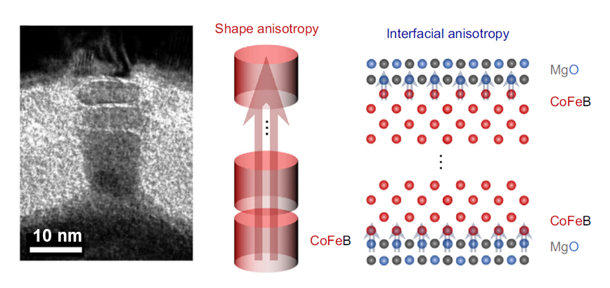
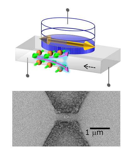
In our laboratory, we are engaged in developing materials and device technologies aimed at further improving the performance of MRAM based on spin-transfer torque (STT), which began to be commercialized around 2018. We are also actively exploring the control of magnetization based on spin-orbit torque (SOT) and electric-field effects—promising candidates for future practical applications—as well as the development of materials necessary for these technologies. Our achievements include a demonstration of the world’s smallest magnetic tunnel junction (MTJ) with a minimum size of 2 nm (left figure), and the proposal and demonstration of SOT-induced switching capable of controlling magnetization down to 0.2 ns (right figure). We also demonstrated the world’s first SOT-MRAM chip using this method, in collaboration with the Center for Innovative Integrated Electronic Systems (CIES) and the Hanyu Laboratory at the Research Institute of Electrical Communication at Tohoku University.
[References (original papers, tutorial papers, and press releases]
- S. Fukami, T. Anekawa, C. Zhang, and H. Ohno, “A spin–orbit torque switching scheme with collinear magnetic easy axis and current configuration,” Nature Nanotechnology, 11, 621-625 (2016).
- J. Igarashi, B. Jinnai, K. Watanabe, T. Shinoda, T. Funatsu, H. Sato, S. Fukami, and H. Ohno, “Single-nanometer CoFeB/MgO magnetic tunnel junctions with high-retention and high-speed capabilities,” npj Spintronics, 2, 1(1)-(9) (2024).
- Press release (2016/03) “A new-structure magnetic memory device developed”
- Press release (2024/01) “Tailoring to Various Applications with Single-nanometer Magnetic Tunnel Junction Technology”
2. Stochastic and Analog Devices for Novel Computing Paradigms
Probabilistic bits, which probabilistically fluctuate between 0 and 1, and analog bits, which take continuous values between 0 and 1, have attracted attention as future computing technologies capable of efficiently performing AI task, combinatorial optimization, etc.
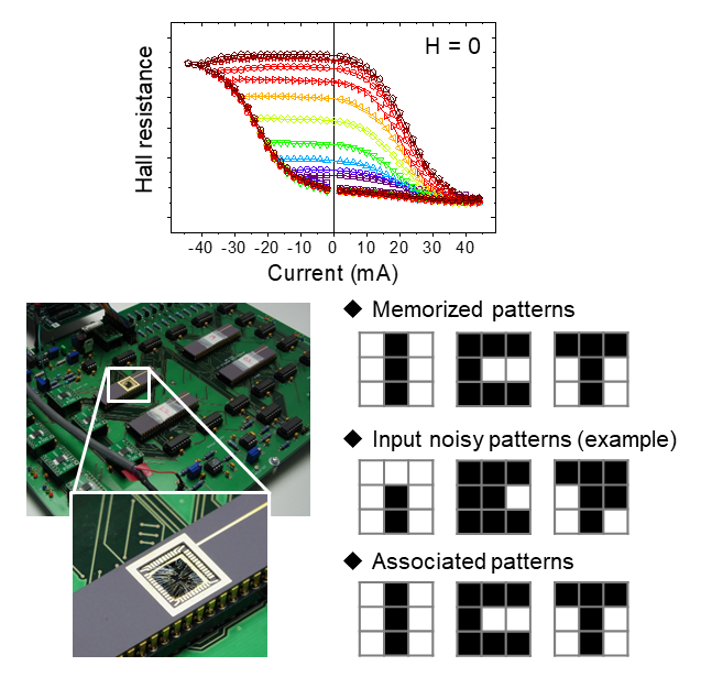
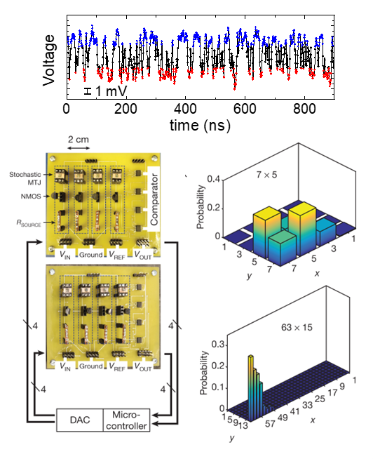
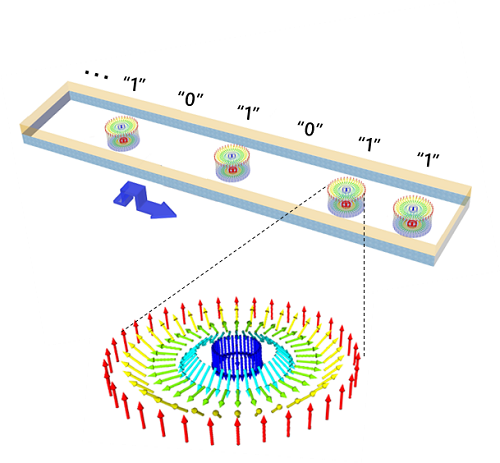
Our laboratory is developing innovative devices that harness thermal fluctuations of magnetization and nanoscale magnetic textures. We are also working on proof-of-concept demonstrations of probabilistic and neuromorphic (brain-inspired) computing based on such devices. Our achievements include the discovery of analog memory functionality in an antiferromagnetic/ferromagnetic structure, and the world’s first demonstration of spintronics-based artificial intelligence hardware using a Hopfield network (proposed by 2024 Nobel Laureate in Physics, Dr. John Hopfield) (left figure). Additionally, we successfully demonstrated the world’s first probabilistic bit and computer using superparamagnetic tunnel junctions, which enable ultra-low-power random number generation (right figure). We are also working to enhance the performance of these technologies and to pave the way for their implementation by delving device physics and improving device performance.
This research is partly conducted in collaboration with Purdue University, UC Santa Barbara, and Sato Laboratory at the Research Institute of Electrical Communication at Tohoku University.
[References (original papers, tutorial papers, and press releases]
- S. Fukami, C. Zhang, S. DuttaGupta, A. Kurenkov, and H. Ohno, “Magnetization switching by spin–orbit torque in an antiferromagnet–ferromagnet bilayer system,” Nature Materials, 15, 535-541 (2016).
- W. A. Borders, A. Z. Pervaiz, S. Fukami, K. Y. Camsari, H. Ohno, and S. Datta, “Integer factorization using stochastic magnetic tunnel junctions,” Nature, 573, 390-393 (2019).
- Press release (2016/12) “The world’s first demonstration of spintronics-based artificial intelligence”
- Press release (2019/09) “”Poor-man’s q-bit” based on spintronics can solve quantum problems at room temperature”
- Press release (2021/03) “Demonstrating the World’s Fastest Spintronics p-bit”
3. Materials and Spin Properties for Quantum Computing/ Sensing/ Communication
Quantum computers are attracting growing attention as a means of delivering the massive computational power required in the IoT and AI era. Among the various systems proposed for realizing quantum bits (qubits), spin-color centers—such as nitrogen-vacancy (NV) centers in diamond—are a promising candidate. These qubits use electron spins as information carriers and are particularly notable for their ability to operate at room temperature and retain quantum information for a long period.
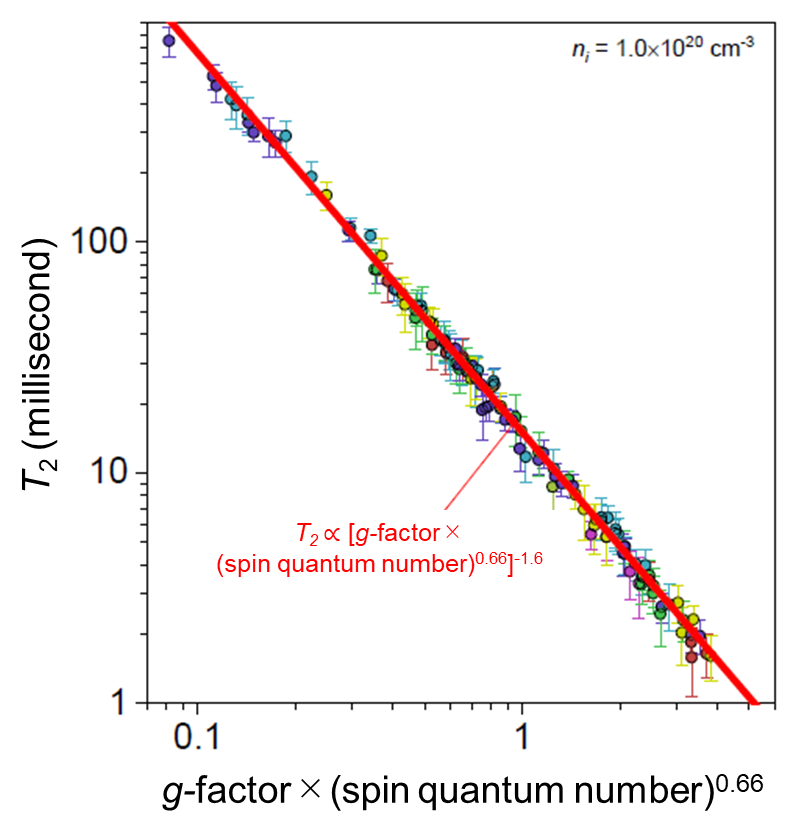
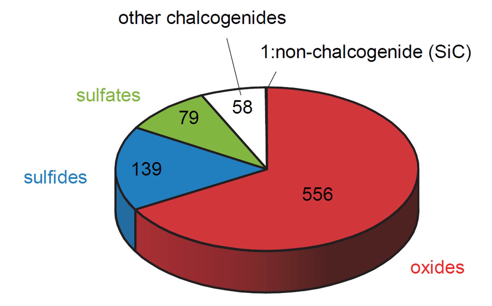
Our laboratory is conducting research to discover and demonstrate color centers in a variety of host materials, including alternatives to diamond. In recent years, we successfully discovered a new type of spin defect in oxide spinels and demonstrated its potential for quantum information retention (left figure). We also established scaling laws for theoretically predicting the quantum performance of color centers, enabling high-speed screening of tens of thousands of candidate materials (right figure). Looking ahead, these advances are expected to contribute to the development of scalable quantum networks, such as quantum memories. Through collaborative research with institutions such as the University of Chicago and Argonne National Laboratory in the United States, we are driving forward technology development from both quantum materials and quantum device perspectives.
[References (original papers, tutorial papers, and press releases]
- G. Wolfowicz, F. J. Heremans, C. P. Anderson, S. Kanai, H. Seo, A. Gali, G. Galli, and D. D. Awschalom, “Quantum guidelines for solid-state spin defects,” Nature Reviews Materials 6, 906-925 (2021).
- S. Kanai, F. J. Heremans, H. Seo, G. Wolfowicz, C. P. Anderson, S. E. Sullivan, M. Onizhuk, G. Galli, D. D. Awschalom, and H. Ohno, “Generalized scaling of spin qubit coherence in over 12,000 host materials,” Proceedings of National Academy of Science of United States of America 119, e2121808119(1)-(8) (2022).
- Press release (2021/04) “A New Guideline for the Solid-state Spin Qubit”
- Press release (2022/04) “A Mathematical Shortcut for Determining Quantum Information Lifetimes”
- Press release (2025/01) “Exploring a new qubit with the gemstone spinel”
4. Novel Spintronic Physics and Functionalities by Innovative Materials
To realize new spintronic devices with outstanding functionality and high performance, the discovery of novel phenomena based on a deep understanding of the underlying physical mechanisms, and the development of materials exhibiting superior properties are essential. Spintronics is still a relatively young research field, and remarkable new phenomena and materials continue to be reported each year.
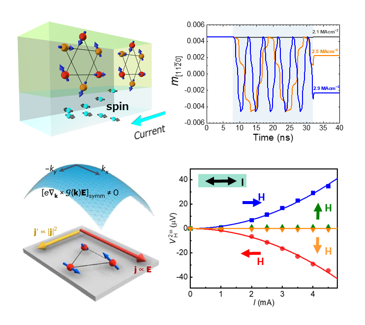
With a long-term perspective on potential future applications, our laboratory aims to pioneer the frontiers of modern condensed-matter physics and materials science by exploring novel spintronic physics, observing emerging phenomena, and developing materials in which such effects become manifest. Our work includes the demonstration of phenomena such as “chiral spin rotation” and room-temperature control of “quantum metric” in non-collinear antiferromagnets that exhibit ferromagnet-like properties due to a topological nature in momentum space, even in the absence of net magnetization. We are also investigating the formation and functionalization of topologically protected spin structures in real space, such as magnetic skyrmions, and developing thin-film fabrication techniques necessary for these studies.
This research is partly conducted in collaboration with Japan Atomic Energy Agency (JAEA), National Institute for Materials Science (NIMS), and Johannes Gutenberg University Mainz (Germany).
[References (original papers, tutorial papers, and press releases]
- Y. Takeuchi, Y. Yamane, J. Yoon, R. Itoh, B. Jinnai, S. Kanai, J. Ieda, S. Fukami, and H. Ohno, “Chiral-spin rotation of non-collinear antiferromagnet by spin–orbit torque,” Nature Materials 20, 1364-1370 (2021).
- J. Han, T. Uchimura, Y. Araki, J.-Y. Yoon, Y. Takeuchi, Y. Yamane, S. Kanai, J. Ieda, H. Ohno and S. Fukami, “Room-temperature flexible manipulation of the quantum-metric structure in a topological chiral antiferromagnet,” Nature Physics 20, 1110–1117 (2024).
- Press release (2019/11) “The First High-speed Straight Motion of Magnetic Skyrmion”
- Press release (2021/05) “A New Spintronic Phenomenon: Chiral-spin Rotation Found”
- Press release (2024/04) “Manipulating the Geometry of ‘Electron Universe’ in Magnets”
5. New Spintronic Application Technologies for Future Information Society
Currently, spintronic technologies are being commercialized in magnetic sensors and non-volatile memory (MRAM), and research and development efforts are advancing toward realizing probabilistic computers, neuromorphic computers, and quantum sensors/memories/communications/computers. However, by utilizing other yet-to-be-explored device functionalities, various new applications will emerge.
In our laboratory, we also conduct foundational research aimed at realizing new spintronic applications that contribute to the advancement and energy efficiency of the information society. One example is a spintronic device designed to meet specific conditions, which outputs RF signals in response to a DC input, and DC signals in response to an RF input. The former function can be used as a signal source for wireless communications, reservoir computing, and Ising computation, while the latter function can be applied as an RF signal detector or for energy harvesting from radio waves in wireless communications. Indeed, we have successfully demonstrated energy harvesting from Wi-Fi band rf signal.
This research is partly being conducted in collaboration with Åkerman Lab at the University of Gothenburg (Sweden) and Tohoku University, the National University of Singapore, and the University of Lorraine (France).
[References (original papers, tutorial papers, and press releases]
- M. Zahedinejad, H. Fulara, R. Khymyn, A. Houshang, M. Dvornik, S. Fukami, S. Kanai, H. Ohno, and J. Åkerman, “Memristive control of mutual spin Hall nano-oscillator synchronization for neuromorphic computing,” Nature Materials 21, 81–87 (2021).
- R. Sharma, T. Ngo, E. Raimondo, A. Giordano, J. Igarashi, B. Jinnai, S. Zhao, J. Lei, Y.-X. Guo, G. Finocchio, S. Fukami, H. Ohno and H. Yang, “Nanoscale spin rectifiers for harvesting ambient radiofrequency energy,” Nature Electronics 7, 653-661 (2024).
- Press release (2020/10) “A New Ultrafast Control Scheme of Ferromagnet for Energy-Efficient Data Storage”
- Press release (2021/11) “Memristive Spintronic Neurons: Combining Two Cognitive Computing Nano-elements into One”
- Press release (2024/08) “Turning Unused Signals Such as Wi-Fi into Energy for Electronics”